
In the fast-paced world of technology, time is more than just money - delays in bringing a product to market can mean the difference between success and failure. A late-to-market product is often at a significant competitive disadvantage that even superior capabilities cannot overcome. Who remembers the Zune these days? Its wireless song sharing and color display in an era on monochromatic iPods were not enough to dislodge such a strong incumbent. First mover advantage matters immensely, with customers typically gravitating towards market leaders, leaving latecomers struggling with lower-tier customers and forced to compete on price.Unfortunately in the semiconductor industry, long design cycles are the norm. And while the entire industry is at the mercy of long design cycles, they are particularly challenging for startups.
The semiconductor industry is characterized by yearslong and lengthening development cycles.
Sophisticated Design Requirements: Chips are becoming increasingly complex, integrating billions of transistors into tiny space - Apple’s M2 Ultra chip packs in more than 130B transistors. Designing for such a complex piece of hardware requires immense precision and takes considerable time to perfect.
Serial Development Process: Traditional chip development follows a serial path—architecture, microarchitecture, design, verification, prototyping, bring-up, validation and then volume manufacturing. This "serial" method of development means each phase must be completed at a high quality level before moving on to the next, leading to accumulated risk of long delays. If you commit a mistake in one phase of this serial process and the mistake is caught on another phase down the line, the serial process must repeat again. This serial method of chip development is a natural way the industry has evolved due to multiple factors. One such factor is that the expertise for each phase is different. For example, a verification engineer is not able to test the design correctness unless the design is complete. A Design For Test (DFT) engineer cannot engage to add his/her value until the design is mature enough where the test insertions are capturing proper events. Our industry relies on design review processes and documentation to ease our way through these phases and reduce miscommunications and mistakes along the way. But these methods don’t always work effectively.
Rising Development Costs: Chip development has become extremely expensive - Qualcomm alone spent close to $8.9 billion on research and development (R&D) in 2024. For startups, raising enough funding to cover the long development process is a near-impossible task, with harsh consequences for startups. The long time-to-market and high development costs mean that no semiconductor startup can undertake a project without significant funding—often in the range of $100 million or more.
Investors are aware of the high funding requirement so the traditional way of getting off the ground by raising friends and family funds or sophisticated angel investors are closed off. Even within large companies, betting on a new market or an aggressive design can have dire consequences and hence is avoided by less innovation-minded leaders. As a result, except for hype cycles, most semiconductor start-up ideas die on the vine and others are typically acquired by a few giant companies. In fact, VC investment in U.S. semiconductor startups has been declining since 2000. See below:
Rolling back the clock to the early 1980s, we saw a much broader participation in the semiconductor development process - like silicon valley’s legendary pioneers Fairchild Semiconductor, Mostek, RCA Semiconductor and Zilog, all of whom have fallen by the wayside or been absorbed in larger conglomerates. In today’s semiconductor world, power is concentrated in the hands of the few players like Intel, nVidia, Qualcomm, and TSMC.
While some semiconductor startups have gained traction in AI and quantum computing, they are by far the exceptions. Most startups are weighed down by the enormous cost and time investment required to bring a new chip to market. Innovators in the IP design segment are experiencing the effect of this pyramid dominated by the few large companies less open to risk taking. The IP houses are expected to be a cycle or two ahead of the big companies who would only use these IP blocks if they are fully vetted in silicon on the same node as the intended target device.
Long development cycles bring another challenge: the uncertainty of future market demands. Chip developers must make decisions years ahead of a product's release, gambling on what features and capabilities will be in demand when the chip finally reaches the market. The need for these changes could come from market dynamics or Industry standards such as IEEE, ITUT, and many consortiums that are built by groups of companies to develop how various interfaces can connect and communicate with each other between chips and across systems. As an example, say you are developing a chip with PCIe interfaces with the 5th generation of this specification prevalent in the market, but you know that PCI-SIG (a group of 900 companies that maintains and develops the PCIe specification) is developing the next generation with more bandwidth and new capabilities to be published a year or two from now. What do you do? You will be tempted to reduce the obsolescence risk of the product you have not even finished designing, by including contingencies that “might” occur when the new spec is released perhaps even before your chip is ready for production.
To hedge against potential market and technology changes, companies often overload their chips with extra capabilities—more programmability, more power, more memory, and more features “just in case”. This approach leads to bloated designs that consume more resources, cost more to develop, and are less efficient. It's a gamble that sometimes pays off, but more often results in costly delays and failed products.
Parallel Development: One potential solution is to adopt a more agile, parallel development model, borrowing from the software industry. Instead of waiting for each phase to finish before starting the next, multiple stages of the development process could run simultaneously. This could drastically reduce the time-to-market and allow companies to respond more quickly to technological changes and market demand.
Modular Design: Another approach could involve modular chip designs. By creating chips with interchangeable components, companies could more easily adapt to shifts in the market without starting the entire design process from scratch. Lately the industry has adopted 3D stacking of dies to reduce the size of each single chip in the chip set in order to increase the yield and lower the cost of the total solution. Similarly some use chiplets to partition various cores and interfaces such that a change in one section of the design, does not require a total redesign of a massive chip.
Operating Systems: Early software pioneers used to write code that ran on bare metal. Software did not only have to deliver a useful application and user experience, but it also had to manage resources such as memory, program counters, and peripherals. As early as the 1950s with IBM’s GM-NAA I/O, and popularized in the 1970s with the introduction of UNIX, software engineers learned that it is beneficial to introduce standardized operating systems that managed resources for applications, including schedulers for running multiple programs concurrently, and libraries of tools and functions for networking, security, and more. By comparison, hardware design would greatly benefit from a similar concept, allowing engineers to focus on creating new features rather than having to worry about organizing and managing chip resources.
In my previous blogs on semiconductors, An Industry at the Precipice and From a Run to a Walk to a Crawl?, I discussed the challenges facing our industry from shortage of trained design engineers to the high cost of chip development to the long development cycles and its impact on the economic viability of the chip design project. The question facing us is – what can we do about it? I believe the era of incremental improvements in each aspect is over. The challenges are getting bigger and the consequences more dire.
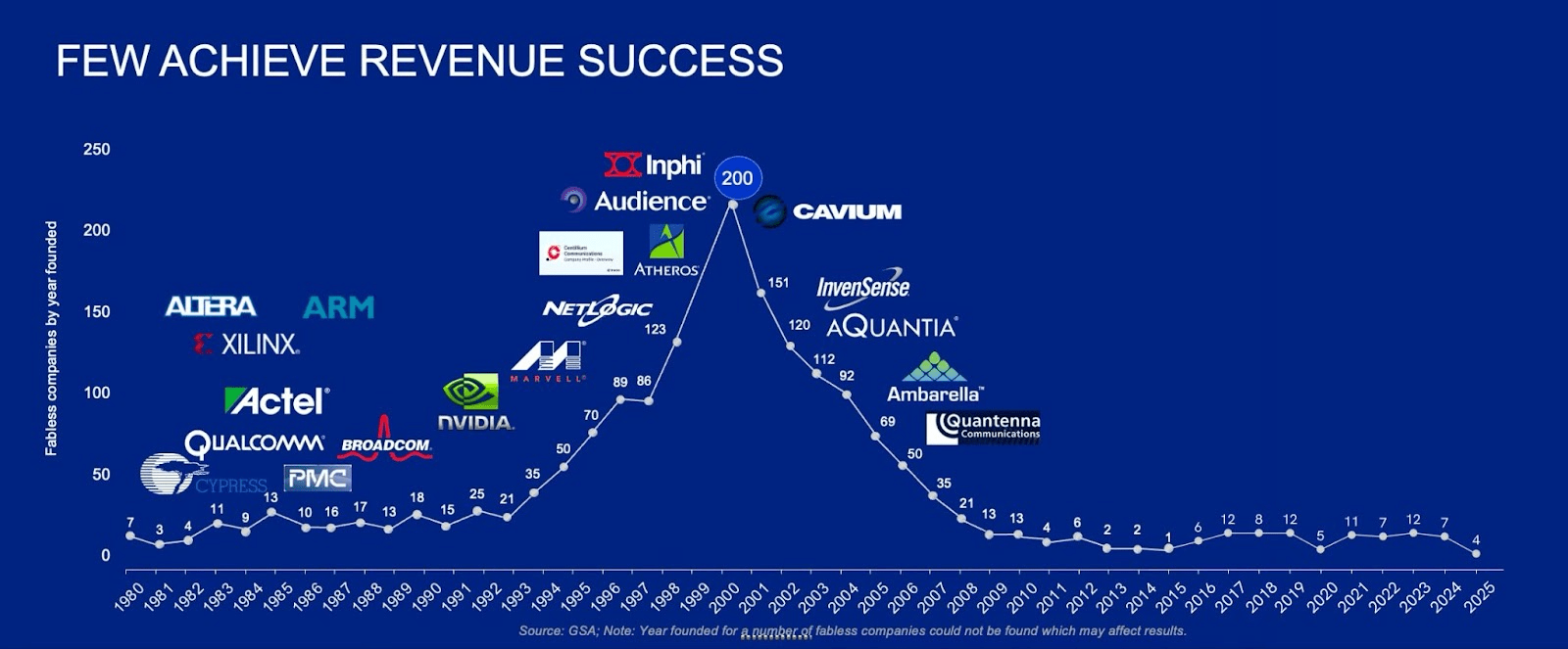
It is clear that a vibrant and growing industry needs constant innovation and the investment affordability in innovation cannot be the purview of a few large players. If you look back at the history of how we got here, nVidia was able to build an entire new business with $20M of investment starting in 1993 over a few rounds before going public. My first startup, Centillium Communication raised $50M as a private company. When we went public in 2000, we still had $17M of that money in the bank. By the time we took Aquantia public in 2017, we had raised nearly $200M. The trend line is not in favor of a vibrant innovative industry.
With the onset of Generative AI, we have a unique opportunity to proactively pursue disrupting the status quo and revitalize our industry once again.
Where do we go next?